

Does your company have requests like these?
We want to
- understand the control methods used in newly released products
- investigate material composition and physical structure of PCBs
- investigate the mounted components and their production costs
- Observation of board configuration from the side by X-ray
- reproduce PCBs found in equipment whose support has expired or whose replacement is no longer available

Is your R&D engineer tasked with circuit and structural analysis of electronic circuit boards in such cases?
Leave it to LTEC!
We can fulfill these requests with our refined investigative strength!!

This will allow you to dedicate the resources in your company to R&D activities.
- Circuit Analysis of Electronic Circuit Boards
- Circuit Analysis of Electronic Circuit Boards
Option Analysis-1 - Circuit Analysis of Electronic Circuit Boards
Option Analysis-2 - Cost Analysis
Circuit analysis of electronic circuit boards
Circuit analysis of electronic circuit boards
One method for determining the strengths/weaknesses of one’s own company is to conduct circuit analysis of the products of competing companies.
Other purposes include...
- Reproduction of the circuit for a PCB or EOL product of one’s own company for which design data has been lost
- Cost analysis
- Utilization of patents
Leave it to LTEC!
We respond to your requests with our superior circuit analysis technologies
Our company is capable of flexibly responding and proposing a wide array of analysis services including product procurement, cross section analysis, and material analysis, in addition to the reproduction of circuits, in order to satisfy our customers’ purpose. Please compare our services with those of other companies.
- Images of Each Layer
- Component List
- Component level detail schematic/Block Diagram
- Components Position on the PCB
- Circuit and Layout Cross Reference Viewer Software
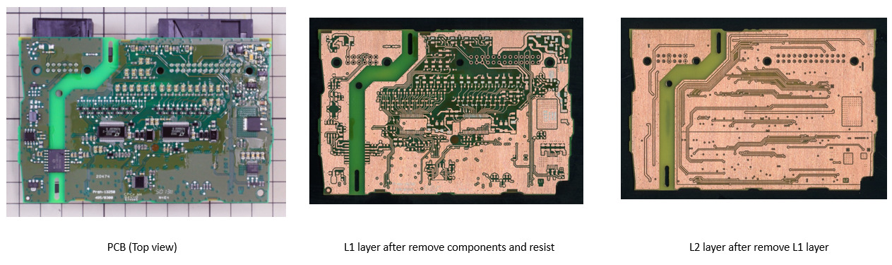
Images of each layer
We can extract circuit schematic diagram and interconnect line/space/thickness, etc. by delayering. The image of each layer is included in a standard analysis report. While most requests are for PCBs of onboard devices, we also have an extensive track record in analyzing high-density mounting PCBs (smartphones), and ceramic PCBs (radio frequency equipment, camera modules). It is also possible to analyze resin encapsulated products, advanced multi-layer products having sixteen buildup layers16-layer boards, 2.5D, 3D integrated products, and chiplet structures. We can investigate operation, components used, circuit/system operation, design ideas, thermal, EMC properties, etc. We are also capable of providing data in Gerber format, DFX format and CAD data such as ODB++, PADS, Cadence, Zuken etc.. (Optional)
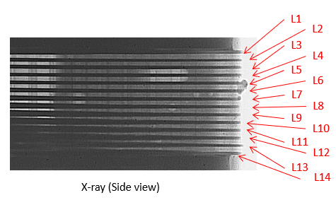
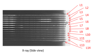
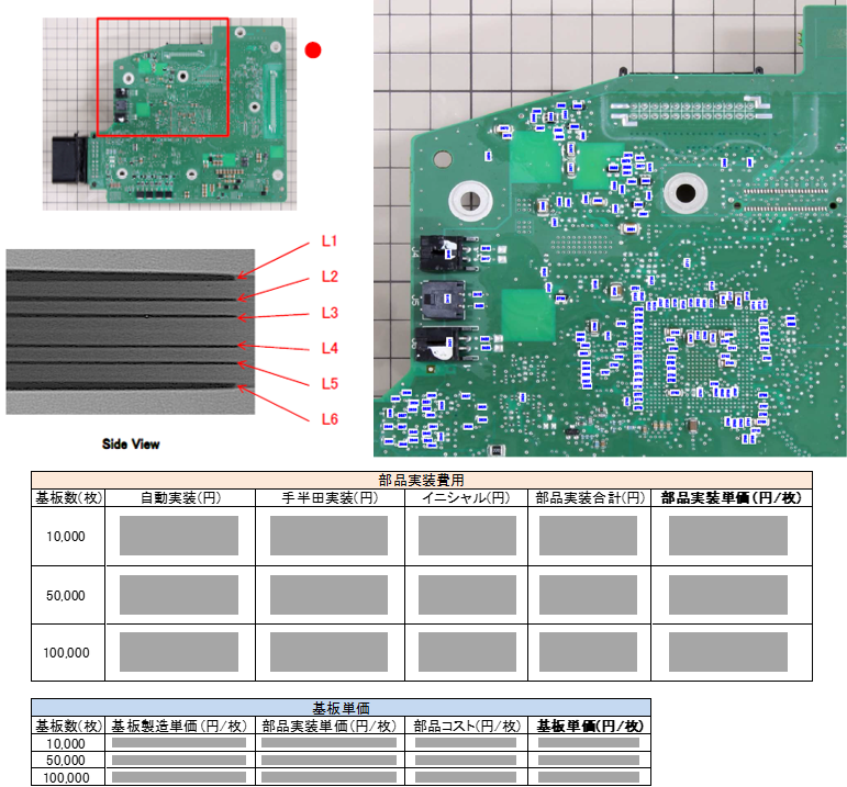
Observation of board configuration from the side by X-ray
You can see that the board configuration has four layers and that the wiring is connected by through holes.
Based on this board configuration information, our "craftsmen" will carefully remove the film as shown in the above picture.
COMPONENT LIST
We can investigate the parts that we remove from the PCB and identify the part number and element constant (L,C,R).
We also accept requests to obtain only the component lists for the purpose of cost analysis.
Since the part number is shared with those on the “schematic” and “mounted part position,” we can confirm the part specifications, how a circuit is used, and mounted position on the layout.
While functions can be identified for most ICs thanks to our proprietary database, it may not be possible for unique ICs such as ASIC.
In this case, we offer confirmation of the manufacturer and estimation of the functions by removing the IC chip and conducting chip marking. (Please make a separate consultation.)
The following shows an example of a component list.
| Component No. | Silk indication | Supplier | Function | (Value described on part) /Nominal | Measured value | Remark |
|---|---|---|---|---|---|---|
| 001 | C51 | - | Capacitor | 7.5uF | 7.254uF | |
| 002 | C52 | - | Capacitor | 15uF | 0.024nF | |
| 003 | Q1 | NXP | Transistor: General-purpose transistors, BC807-40W | - | - | cf.datasheet |
| 004 | R21 | - | Resistor | 220ohm | 220.8ohm | |
| 005 | C53 | - | Capacitor | 1uF | 994.1nF | |
| 006 | D41 | - | Diode | - | - | |
| 007 | IC11 | Freescale | IC:RISC MCU Including Peripheral Pin Multiplexing with Flash and Code Compression Options | - | - | cf.datasheet |
| 008 | R22 | - | Resistor | - | - | |
| 009 | IC12 | Infineon | IC:Low-side Switches -Multiple/Channel Additional Low Side Switches | 220kohm | 220kohm | cf.datasheet |
| 010 | IC13 | Infineon | IC:H-Bridge for DC-Motor Applications | - | - | cf.datasheet |
| 011 | C53 | - | Capacitor | 3.9uF | 3.889uF |
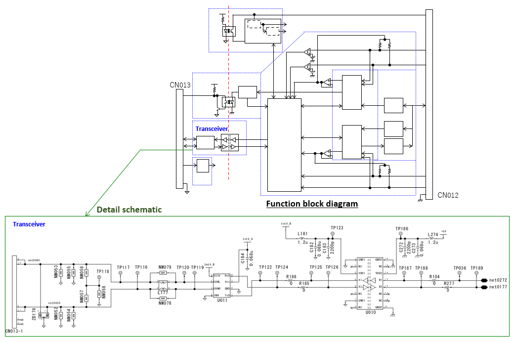
BLOCK DIAGRAM, SCHEMATIC
We can prepare a flat schematic based on the wiring information we extract, and summarize the diagram in terms of functions so that it is easy to determine the operation by determining the power supply node, main route, etc. This is the core process of analysis, where the intention of the designer and the pride of our engineers come into conflict. The output consists of the block diagram which indicates the overall functions and signal flow, and a detailed schematic. If it is sufficient to find the connection information, we can deliver the report as a flat schematic (without summary), and it will be even less expensive in this case. While the PDF schematic and EDIF library data will be provided in the standard service, we can also deliver the information as OrCAD data separately. (Optional)
Examples of a block diagram and schematic are shown below.
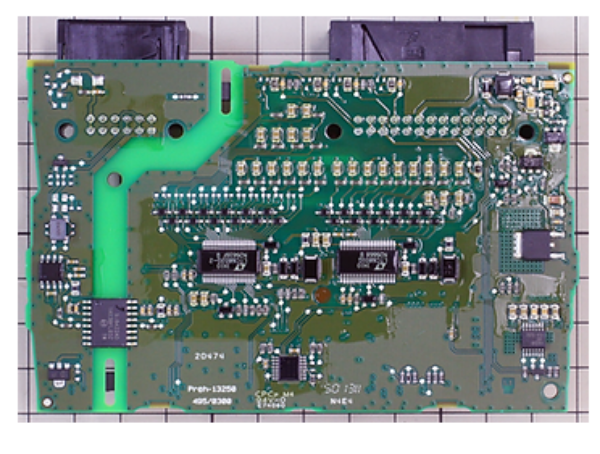
COMPONENTS POSITION ON THE PCB
A common number is assigned for each part on both the component list and schematic to indicate the mounted position for each part.
Since a common part number is used between the “schematic” and “component list,” it is possible to confirm how it is used in the circuit and the part specifications.
In addition, we assign a number to each non-mount point as “NM000” if the point is a Non Mount (NM) so that it is clear that the point is a non-mount even on the schematic. (Standard)
Reflection of test points is optional.
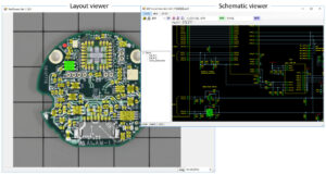
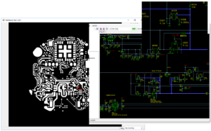
CIRCUIT AND LAYOUT CROSS REFERENCE VIEWER SOFTWARE
While we deliver our report with a drawn schematic, we also provide the Viewer tool developed by LTEC Corporation. You can use this Viewer tool to trace the interconnect path in each physical layer of the PCB and cross-reference each component to the schematic.


Circuit analysis of electronic circuit boards Optional analysis-1
- Inductance Measurement
- PCB Pattern Line and Space Measurement
- Layout Data Creation of Each Layer
- PCB Cross Section Analysis
(Layer Composition) - PCB Cross Section Analysis
(Material Composition Analysis)
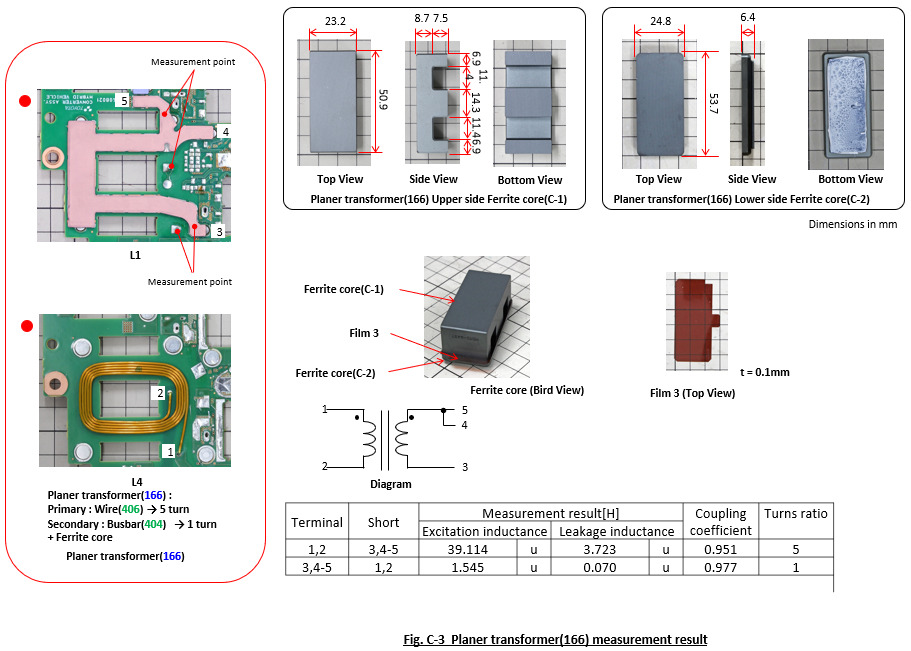
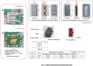
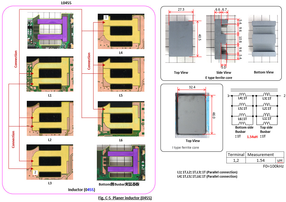
INDUCTANCE MEASUREMENT
-
We can measure the excitation inductance, leak inductance, and coupling coefficient (k) of mounted transformers, and the wiring width in transformers using the calculated PCB wiring with a winding ratio after circuit analysis.
*An additional product may be required. We will discuss with customer in advance.
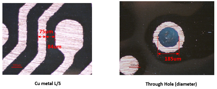
PCB PATTERN LINE AND SPACE MEASUREMENT
We can make clear the design rules for the analysis subject by taking more detailed measurements on the PCB plane. The following shows an example of PCB pattern line and space measurement.
Plane measurement result
- Minimum wiring width: 75um
- Minimum wiring interval: 84um
- Minimum TH inner diameter: φ0.185mm
LAYOUT DATA CREATION OF EACH LAYERS
- For the purpose of magnetic field simulation and impedance calculation, we can convert the wiring image for each layer (bitmap data) into CAD data. We support the following formats: Gerber, DXF, PADS, ODB++, Cadence, Zuken (CR)
CAM interface tools that support ODB++
1. Altium: PROTEL, P-CAD, Altium Designer
2. Cadence: Allegro PCB Design, Cadence OrCAD PCB Designer
3. First: START
4. Mentor Graphics: Board Station, Expedition, SFX J-1, Power PCB
5. YDC: CADVANCE --II & I1I
6. Zuken: CR5000 / PWS, CR-5000 / BD, Visula
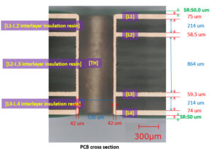
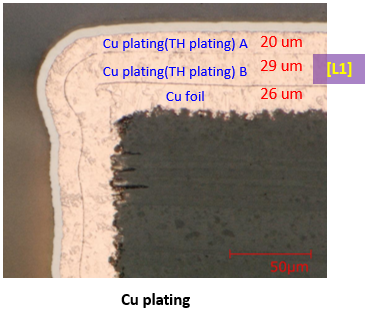
PCB CROSS SECTION ANALYSIS
We can make clear the detailed PCB structure through observation of the PCB cross section. In cross section analysis, we partially cut out the PCB by selecting a location that will not affect circuit analysis. By processing after cutting the cross section, we can make the copper foil and TH plating layer more apparent, and count how many times TH plating has been conducted and measure the plating film thickness. Recent onboard power supply PCBs show a trend for a thicker copper foil thickness in order to ensure heat radiation and reduce the parasitic resistance. The following shows an example of layer composition.
An example of layer composition
Example of layer structure


Matrial analysis example
| Layer structure | Thickness(µm) | |
|---|---|---|
| Solder resist | resin | 50 |
| L1 | Copper plating (TH plating) layer A | 20 |
| Copper plating (TH plating) layer B | 29 | |
| copper foil | 26 | |
| L1-L2 interlayer insulating layer | Resin + 1 glass cloth | 214 |
| L2 | copper foil | 58.5 |
| L2-L3 interlayer insulating layer | Resin + 5 glass cloths | 86.4 |
| L3 | copper foil | 59.3 |
| L3-L4 interlayer insulating layer | Resin + 1 glass cloth | 214 |
| L4 | Copper plating (TH plating) layer A | 20 |
| Copper plating (TH plating) layer B | 28 | |
| copper foil | 26 | |
| Solder resist | resin | 50 |
| Through hole inner thickness | Plating layer A + B | 42 |
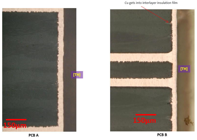
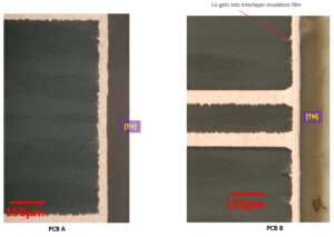
This is the enlarged image of the through hole (TH) part of a PCB. Compared to PCB A, infiltration of TH plating into the interlayer insulating resin is observed in PCB B.
This occurs as the glass cloth expands when the TH is opened and Cu plating enters during TH plating. If this occurs to a severe degree, it may cause a short circuit in a dense pattern or ion migration depending on the environment of use (mainly due to moisture).
Cross section analysis is an effective method to confirm the degree of finishing in a product.
PCB MATERIAL ANALYSIS
We can conduct material composition analysis on resins, solder resist, etc. that are used between the layers of a PCB. Additives are contained in resin PCBs other than resins for the purpose of adding strength and fire retardancy. While there are several measurement methods, we use different methods depending on the purpose as follows in a rough summary.
- Resin main component: FT-IR
- Additive: EDX
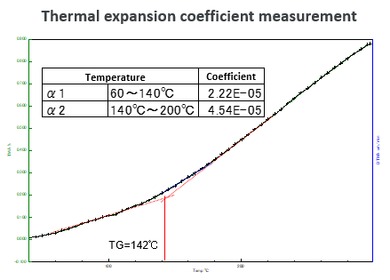
It is also possible to conduct thermal expansion coefficient measurement for reference on how much a PCB expands under the actual environment of use (high temperatures).
- Linear expansion coefficient measurement: Thermomechanical analysis (TMA)
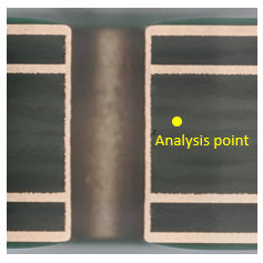
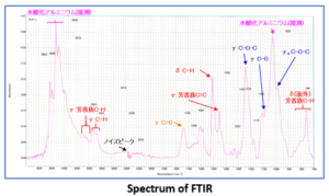
An example of PCB resin analysis with FT-IR

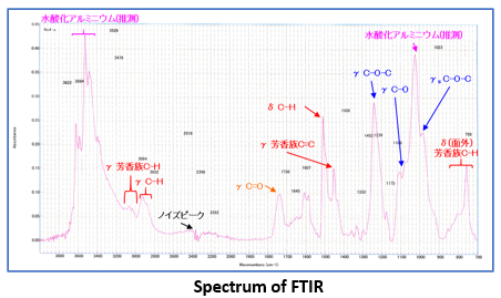
| Peak | Attribution |
|---|---|
| Around 740-850 | δ (out-of-plane) CH: aromatic ring |
| Around 1000 | γs, COC: Aromatic Ether |
| 1023 | Aluminum hydroxide |
| 1106 | δ CO: Ether |
| 1239 | γAs, COC: Aromatic Ether |
| 1452 | γ C=C: aromatic ring |
| 1508 | δ CH |
| 1736 | γ C = O: carbonyl group |
| 2873〜2963 | γ CH |
| 3037〜3064 | γ CH:aromatic ring |
| 3476〜3622 | Aluminum hydroxide |
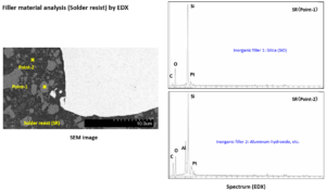
An example of filler material analysis (solder resist material analysis)

An example of thermal expansion coefficient measurement
- Linear expansion coefficient measurement on a PCB using thermomechanical analysis
This case indicates that the glass transition temperature TG (inflection point) is around 142°C.
Circuit analysis of electronic circuit boards Optional analysis-2
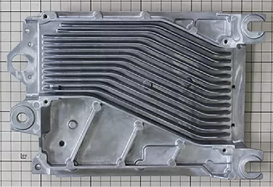
HEAT DISSIPATION ANALYSIS
We can estimate the temperature distribution based on the results of circuit analysis (estimation of heat sources), heat transfer paths, and the shape and material of radiators. It can be used in finding out how much of a temperature margin has been allocated and what creative points they adopt.
The following shows an example of temperature distribution by heat dissipation analysis.
An example of temperature distribution
- A radiator for an onboard power supply module
Air guiding fins are formed to help the air blow from the cooling FAN.
The element and PCB, which are the heat sources, are installed on the back side.
- Temperature distribution simulation results on a heat radiation mechanism
Heat generation from the rectifier diode is larger than the transistor part, reaching 161°C at maximum.
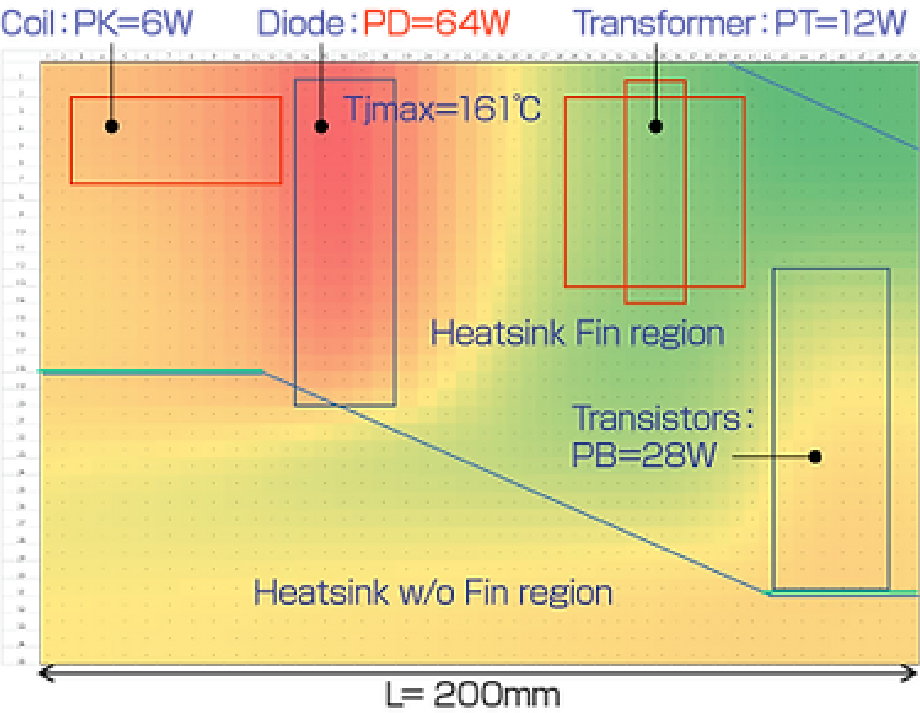
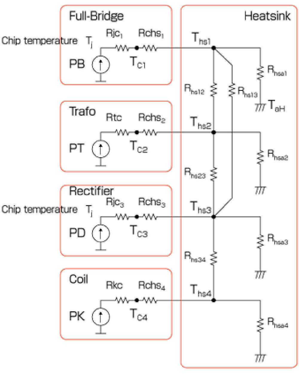
Examination of the temperature rise in parts and components with the application of a heat equivalent circuit.
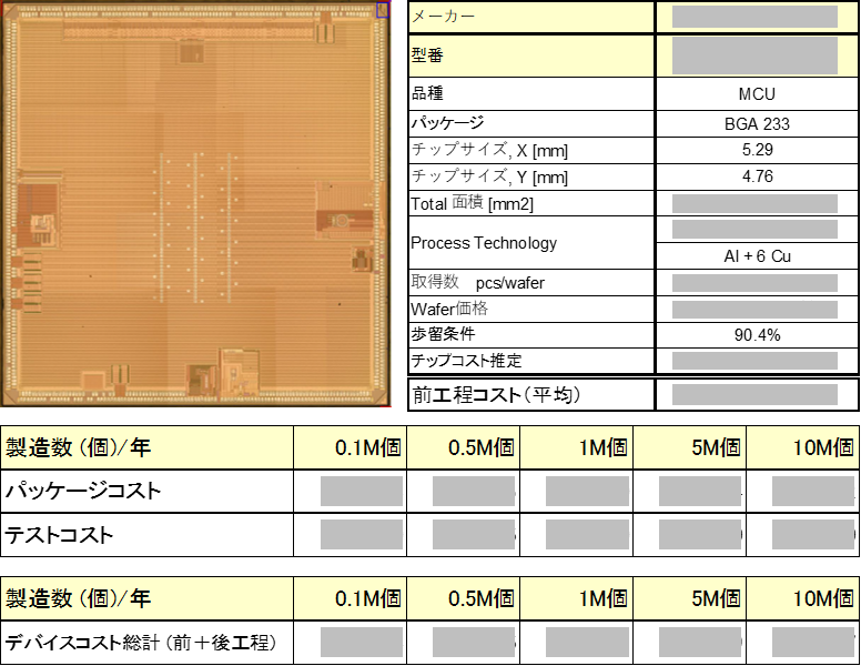
Cost analysis
Cost information is extremely important when creating benchmark reports. Our company generates cost estimates based on a cost accumulation model of mounted parts, PCBs, materials, and production costs. If our customer can specify production quantity and the country of production, we can reflect them in the costs.
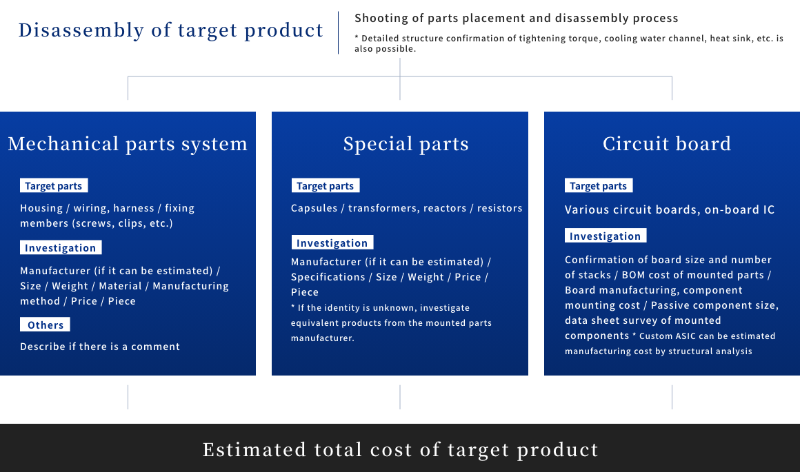
MECHANICAL PARTS 機構部品
- We can estimate the material expense for mechanical part based on the composition of the member, and the processing expense based on the external shape of the estimation subject.
- We can also estimate the costs based on the types and quantity of screws used, the assembly process by analogical inference when the subject is disassembled, as well as sealing materials, etc. also by analogical inference.
ELECTRONIC CIRCUIT BOARD 電子回路基板
- We estimate the manufacturing price of a PCB based on the PCB size, number of laminated layers, production processes (through Via, build-up, etc.), surface protection film (use of HumiSeal), etc.
- We also estimate the production cost of a PCB based on the mounted parts and mounting method (manual mounting, flow soldering, reflow soldering, etc.).
MOUNTED PARTS 搭載部品
- For ICs in existing products and passive components, it is also possible to infer the purchase price by analogy based on characteristics and size. For custom ICs, estimate with equivalent products based on the type and number of terminals, or estimate by presuming the yield based on the chip size of the mounted semiconductor, process, and manufacture Fab (presumed).