

Does your company have requests like these?
We want to
- conduct circuit analysis on an IC and obtain detailed circuit information of the products of competing companies
- estimate the internal functions of ASIC based on the chip layout (floorplan)
- know the process structure and materials used in leading-edge devices
- analyze complex package structures such as image sensors having stacked structures, etc.

Is your design/development engineer tasked with circuit and structural analysis of semiconductor products? If so, ---
Leave it to LTEC!
We can fulfill these requests with our refined investigative strength!!

This will allow you to dedicate your resources to R&D activities.
Semiconductor products we analyzed
- Silicon semiconductors, compound semiconductors
- Power devices, RF devices, ICs (to the minimum size of 14 nm), sensing devices, MEMS
- Various modules (radio frequency modules, power modules, sensor modules)
Semiconductor circuit analysis
IC FUNCTION ESTIMATION
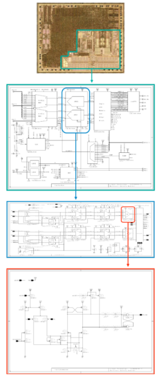
What is IC function estimation?
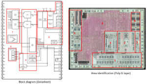
We can identify the details about each block by classifying the types such as analog, logic, memory and IO based on the examination of IC layout.
Function classification and function estimation analyses are recommended for people who want to know the overall chip layout, even though detailed circuit analysis is not necessary, and want to conduct circuit analysis but do not have a sufficient budget.”
1. Function classification
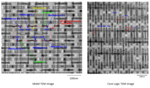
- We classify IC functions a logic, IO, and analog, and calculate area occupancy ratio based on observation of the Gate oxide layer. We identify the standard (STD) cell size for logic and 1 bit cell size for memory through SEM observation of the Gate layer.
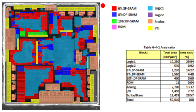

- We identify the standard (STD) cell size for logic and 1 bit cell size for memory through SEM observation of the Gate layer.
2. Function estimation
-
We estimate each function block by identifying the characteristic layout configuration against the block diagram and pin assignment on the data sheet, and obtain the IP area of each block.
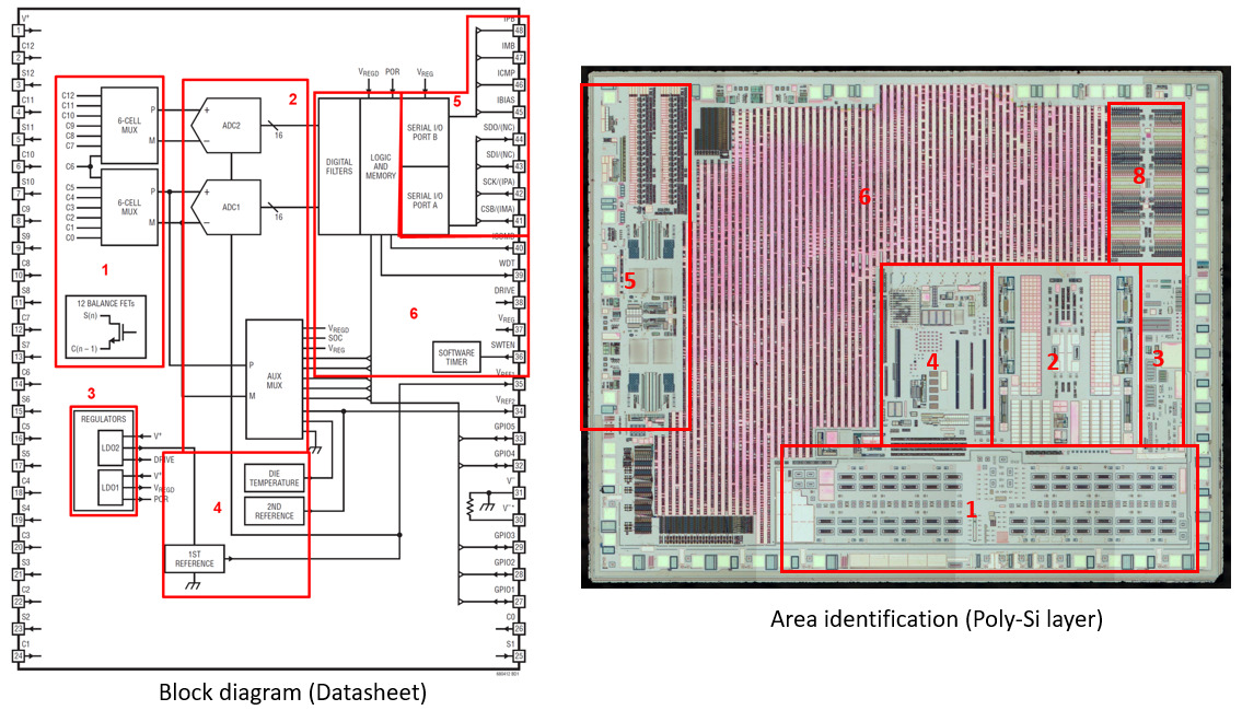
Reason of function block estimation and area size of each blocks
| Block No. | Function | Comments | Area (10^3um^2) |
|---|---|---|---|
| 1 | MUX | It is estimated as 'MUX', because the input terminals related to MUX are connected to this area and it has several identical layout patterns. | 2,370 |
| 2 | ADC | It is estimated as 'ADC', because the signals from 'MUX' are connected to this area and it has two identical layout patterns. | 1,210 |
| 3 | Regulator | It is estimated as 'Regulator', because there are multiple diodes to be consist of bandgap circuit, and big size transistors connected to wide metal patterns. | 450 |
IC CIRCUIT ANALYSIS
“We want to know the circuit configuration of this LSI chip.”
- To understand specific circuit technologies and features of competing products
- To collect evidence for patent license contract negotiations/lawsuits
Leave it to LTEC!
We respond to your requests with our superior circuit analysis technologies
LTEC Corporation utilizes advanced circuit extraction tools and methodologies to reconstruct schematic diagrams from the physical IC layout and organizes them into a logical hierarchical flow. We cover a wide range of manufacturing technologies down to highly advanced process nodes. We also collect product information from specifications, technical documents, etc., to crosscheck validity of our analysis results.
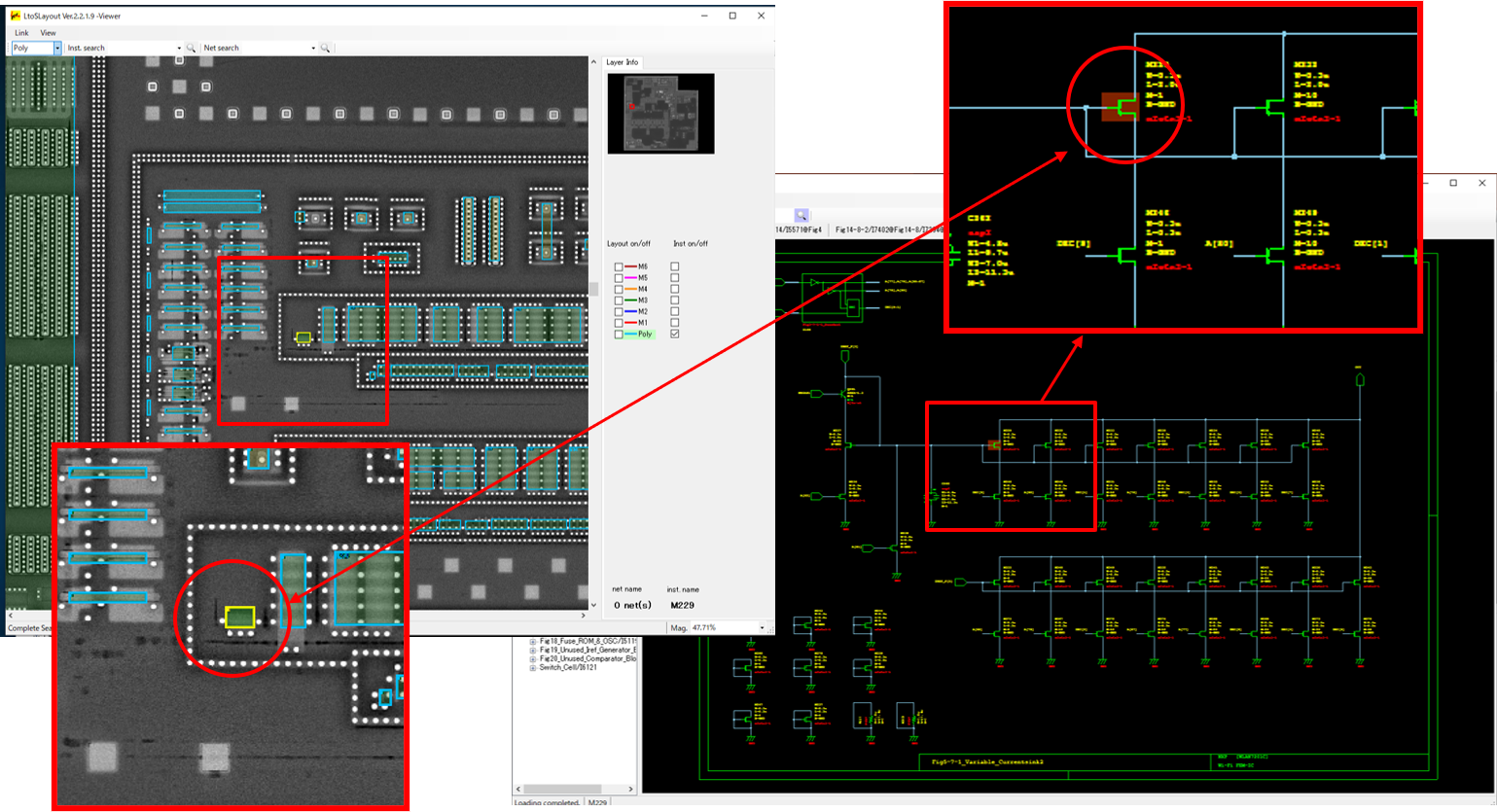
CIRCUIT VIEWER SOFTWARE
-
This software is used to analyze extracted circuit schematics and corresponding reconstructed IC layout patterns of analog/mixed-signal integrated circuits. Some of the key features of this cross-liked hierarchical schematic/layout image viewer are the ability to locate annotated objects of the reconstructed layout in the schematic, highlight connection paths, convert netlists and schematics into industry standard file formats. We offer customer access to this powerful tool.
The circuit viewer is an effective productivity enhancement tool for the development engineer as well as the Intellectual property analyst.
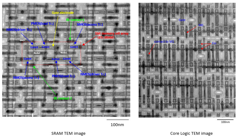
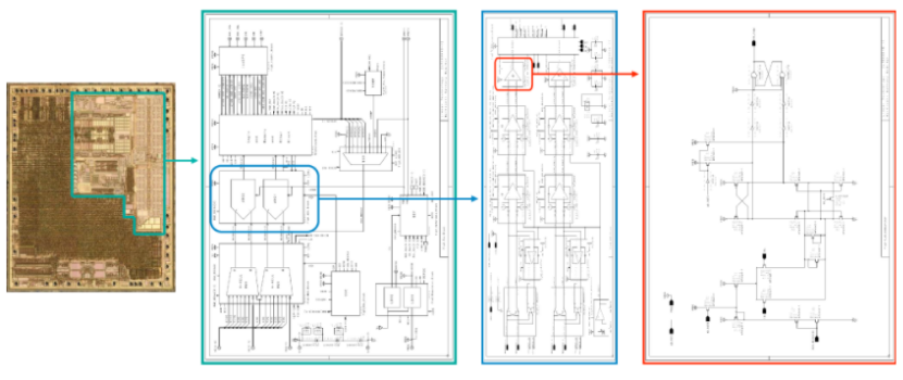
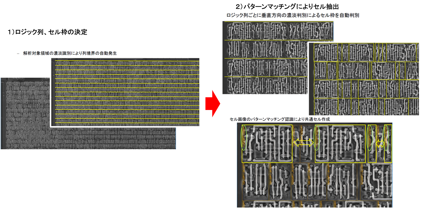
LOGIC CIRCUIT ANALYSIS EXAMPLE
- Unlike analog circuits, logic circuit blocks don’t have a unique appearance. Logic circuits have large number of elements, and all look the same in the IC layout; therefore, they are more difficult to analyze. However, using our layout pattern matching software, even large logic circuits can be analyzed (with the exception of random logic).
Semiconductor circuit analysis
Semiconductors, manufacturing technologies, and packaging technologies continuously evolve. Are you interested in understanding competing technology trends, diverse product portfolios, various product features, etc.? Our company provides flexible analysis services with consistent implementation of everything from product analysis and sample procurement.
1. Structural analysis of printed circuit boards and packages
- X-ray internal structure check
- Analysis of the plane layout and design rules
- Cross-section structural analysis & material composition analysis, etc.
2. Structural analysis of IC chips
- Structural analysis inside a chip such as laminate structure and circuit component elements (transistors, resistors, capacitors, etc.)
- Visualization of internal structures (diffusion layer) of Si die
- Process rule estimation
- Manufacturer identification
3. Subject products
- Semiconductor products: Logic, Analog, LCD drivers, Tag-ICs, power devices, etc.
- Compound semiconductor products: LDs, Power Amps (modules), etc.
- Piezoelectric substances: SAW filters, duplexers, etc.
- LCD panels, organic EL, MEMS, etc.
Reference examples
 |
 |
 |
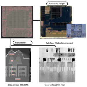 |
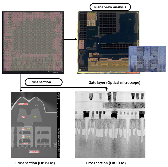
- IC Die Overview Analysis
- Cross-section Analysis
- Layout Analysis
- Material Composition Analysis
- MEMS Analysis
- Power Device Analysis
- Image Sensor Analysis
- IC Package Analysis (Cross Section)
- IC Package Analysis (Plane View)
IC DIE OVERVIEW ANALYSIS
Semiconductors are continuously evolving. Are you interested in understanding competing technology trends, diversifying product portfolios, various product features?
Our company provides flexible analysis services with consistent implementation of everything from product analysis and sample procurement.
Reference examples
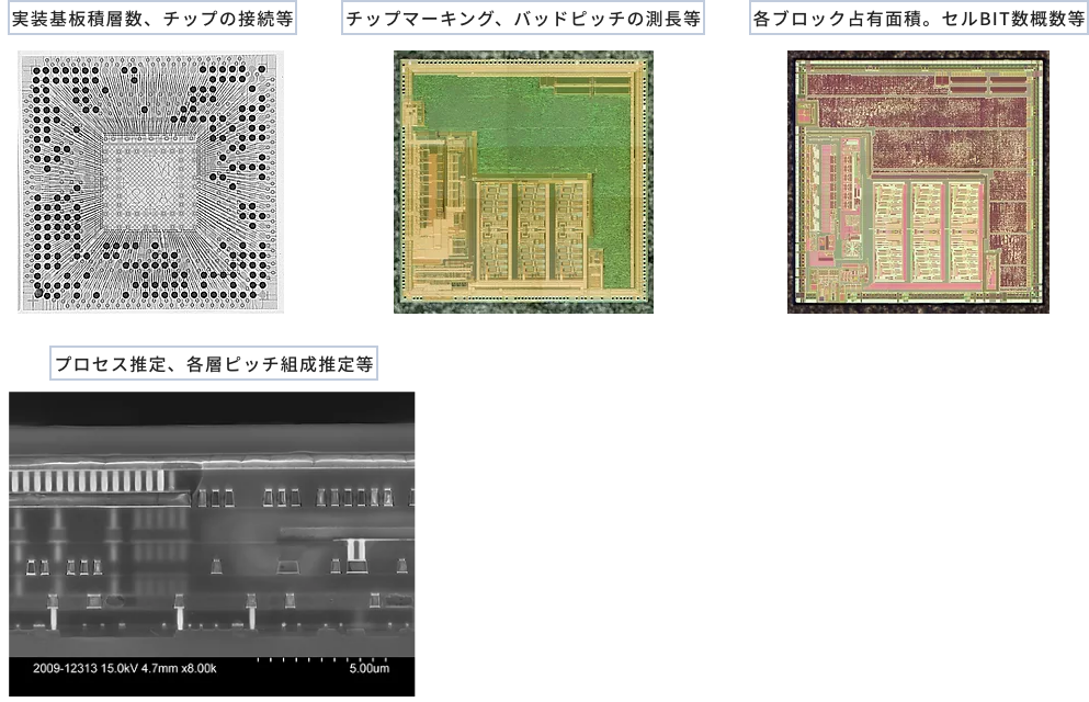
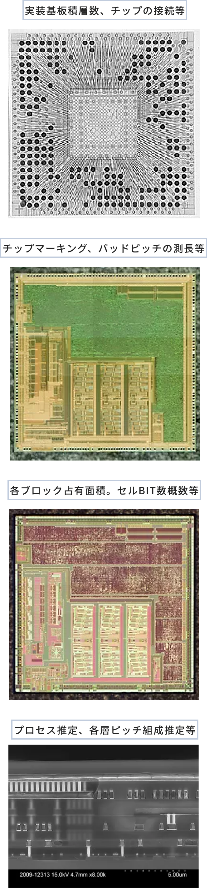
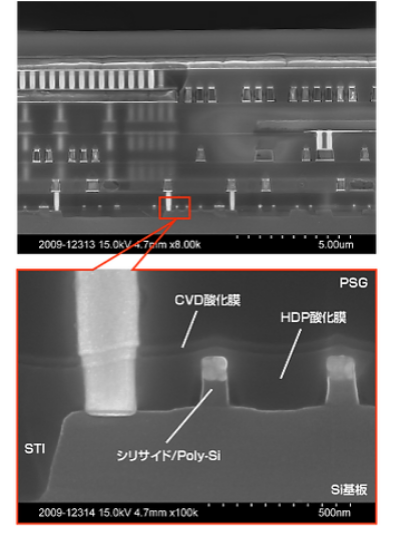
- Package optical and X-ray images, package decap, chip images, die marking.
- We measure the die area of various function blocks and calculate area occupancy rate based on plane view observation of the Gate layer.
- We calculate memory bit number, logic cell numbers, estimate process node and material composition of each layer, etc.
CROSS-SECTION ANALYSIS
Semiconductors are continuously evolving. Are you interested in technological trends found in diversifying competing product portfolios?
Our company provides flexible analysis services with consistent implementation of everything from product analysis and sample procurement.
Reference examples
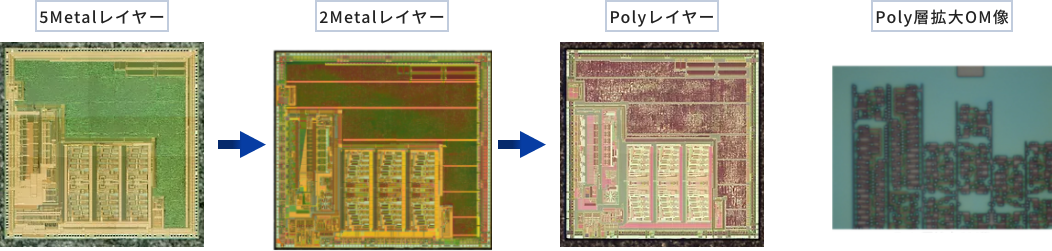
- Structural analysis inside a chip such as laminate structure and circuit component elements (transistors, resistors, capacitors, etc.) and process estimation. (structural analysis using SEM, FIB and TEM)
- Evaluation of the internal structures of Si die using the Si etching solution
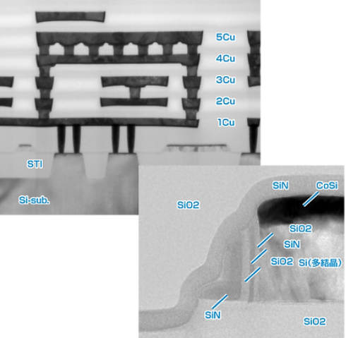
LAYOUT ANALYSIS
Semiconductors are continuously evolving. Are you interested in technological trends found in diversifying competing product portfolios? Our company provides flexible analysis services with consistent implementation of everything from product analysis and sample procurement.
Reference examples
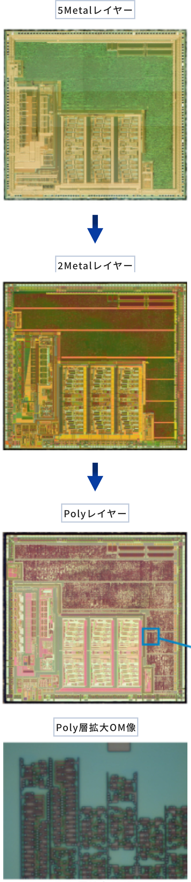
- Analysis of plane layout and design rules by delayering of each layer
- Chip size: 0.3 mm and larger, design rule: We have a track record of 14 nm.
- Wiring: Cu, Al, etc., interlayer film: We have a track record of organic-based, inorganic-based, and low-K films.
MATERIAL COMPOSITION ANALYSIS
Advanced semiconductor products use increasingly diverse materials. The use of thin film analysis tools are indispensable for the evaluation of precision integrated circuits. Due to its ability to suppress disturbance signals, our TEM-EDX equipment is eminently suitable for this type of analysis. We also use SEM and TEM contrast-imaging methods for material composition estimation.
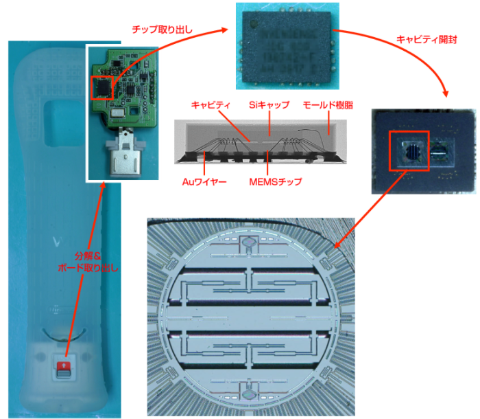
MEMS ANALYSIS
Micro Electro Mechanical Systems (MEMS) have an on-chip driver circuit and a cavity-suspended component. To conduct structural analysis, creative techniques must be used to open the IC package so as not to damage this highly sensitive structure.
Reference examples
- Various acceleration sensors, gyro sensors, SI microphones, pressure sensors, Digital Micromirror Device (DMD), etc.
- Structural analysis on the drive part (film thickness, pitch, etc.), evaluation of the sealing part, connection check on the terminal and drive part, etc.
Example of opening a gyro sensor installed on a game machine
POWER DEVICE ANALYSIS
- Power semiconductors are key enablers of energy saving. They are widely used in household applications such as refrigeration, smartphones, tablets, PCs, TVs, air conditioners, as well as in electric vehicles, photovoltaic power generation, railways, wind power generation, etc.
- Our company performs analysis of a wide variety of products and underlaying technologies including IGBT, RC-IGBT, SIC MOSFET, GaN-HEMT, GaO.
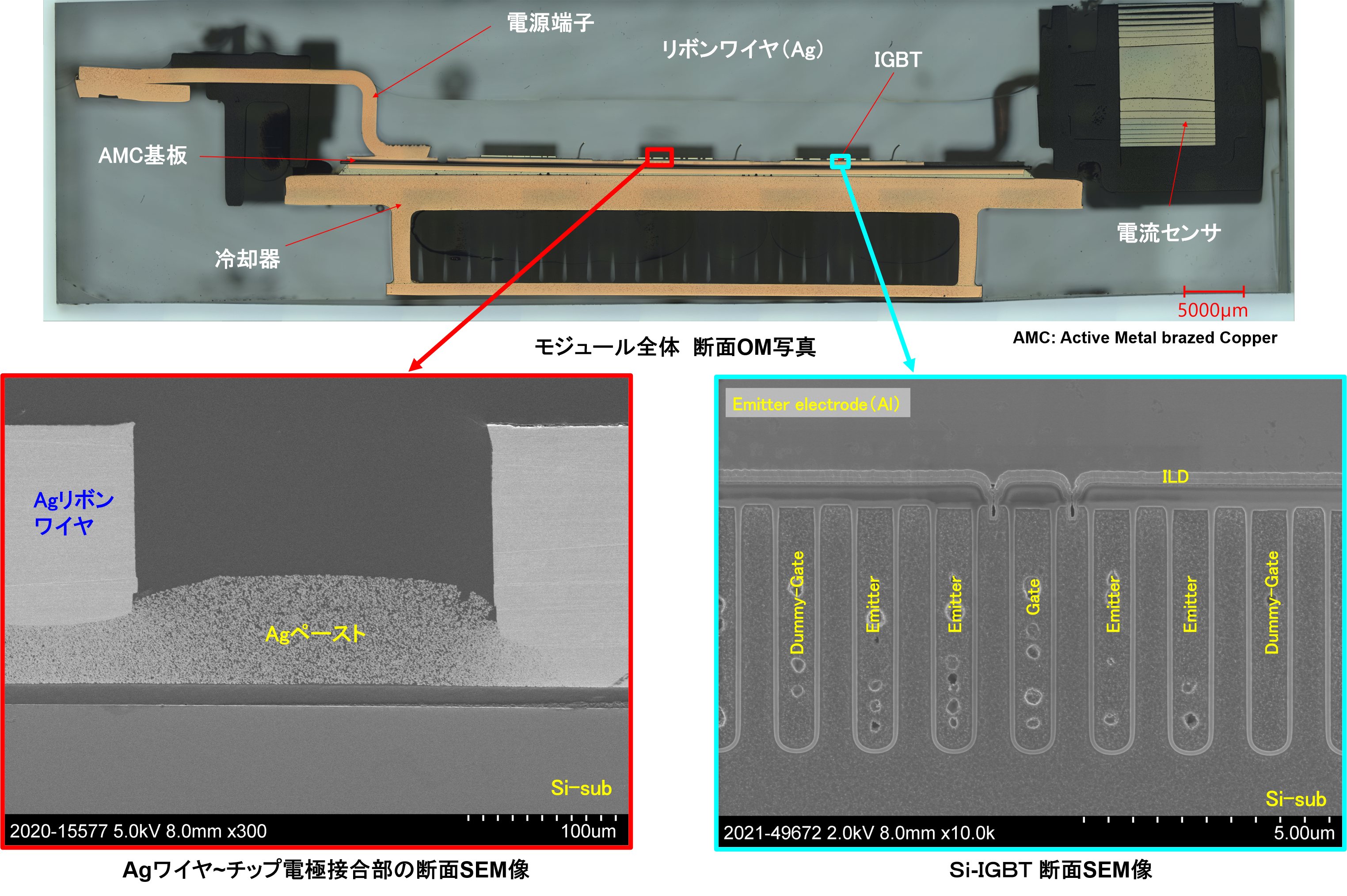
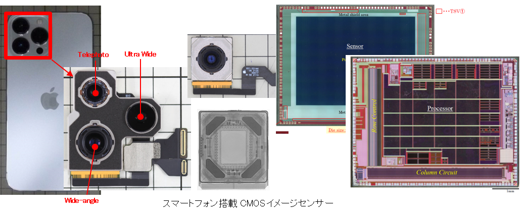
IMAGE SENSOR ANALYSIS
Image sensor technologies installed in digital cameras, drones, cell phones, etc., are continuously advancing to meet the needs for high resolution and high-speed data processing. We perform many different types of analysis tasks from disassembly of the on-board CMOS image sensors of smartphones to the extraction of mounted sensors. We perform many different types of analysis tasks from disassembly of the on-board CMOS image sensors of smartphones to the extraction of mounted sensors. We also analyze highly complex structures such as back-side irradiation image sensors having stacked sensor- and control chips. Our work includes layout-, structure-, and circuit analysis of the lower control IC after removal.
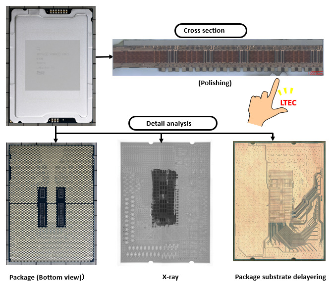
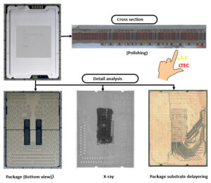
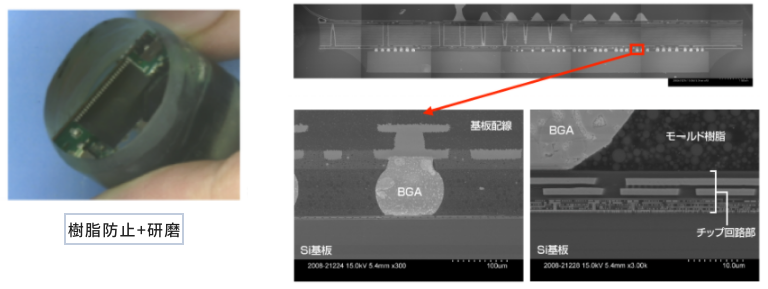
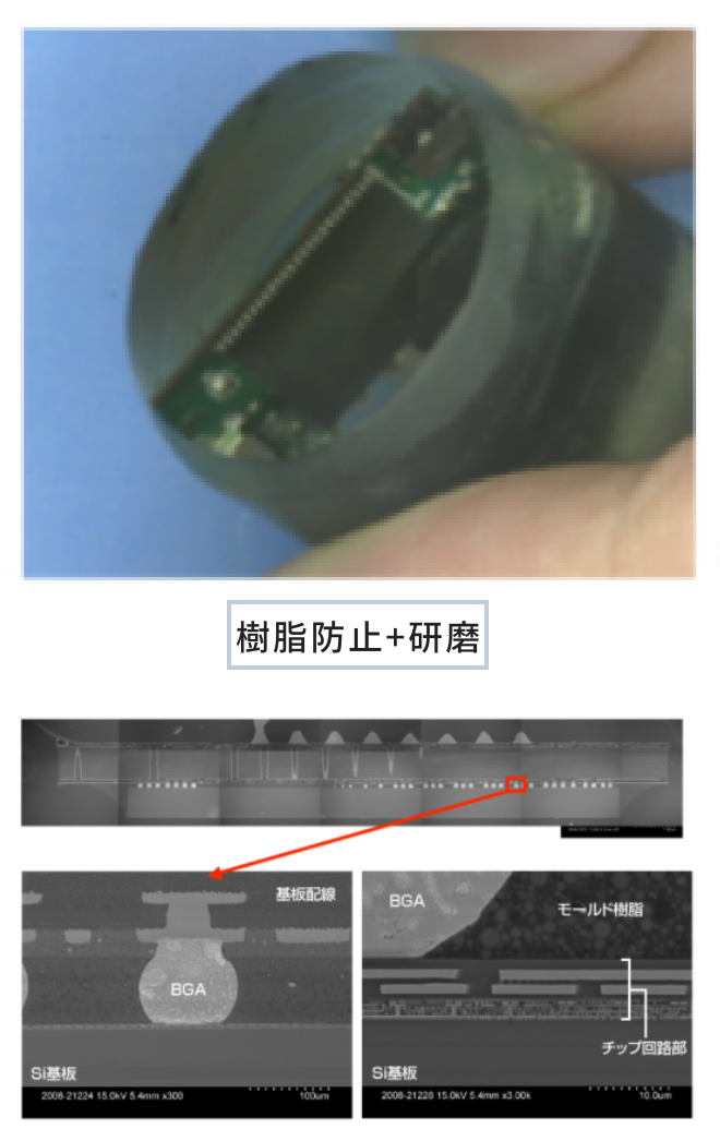
IC PACKAGE ANALYSIS (CROSS SECTION)
2.5 and 3D packaging techniques, active and passive component embedding technologies aim to reduce wiring pitch and increase the number of layers. Conventional cross section observation of various structures having internally mounted TSVs and active/passive elements embedded within PCBs and substrates is typically accomplished by polishing. However, sometimes the sample can get damaged. LTEC developed a special polishing method that allows the repair of partially damaged samples by removing the damaged layers of the polished cross-section. Subsequently, ion beam process is applied to complete the observation. If the damage is more severe, we can use ion beam process instead of polishing, which yields damage-free cross section.
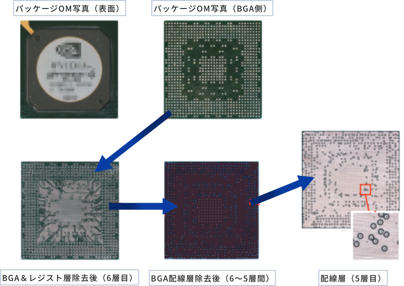
IC PACKAGE ANALYSIS (PLANE VIEW)
While we are able to trace a signal path leading to the package terminal using X-ray, this method is not applicable in case of multi-layer package substrates or complex modules. In those cases, we use delayering method. We also perform design/layout rule analysis, system architecture analysis, etc., by delayering package substrates, modules, various 3D package structures, and create design data in .MCM, pads, CR, or ODB++ formats.
Reference examples
-
Analysis of plane layout and design rules by delayering of each layer
*We have a varied track record including various modules, FC-BGA, LTCC, etc..